

The Silicon Chokepoint: Why the $1 Trillion AI Industry Runs on a Single Dutch Monopoly
Inside ASML’s Extreme Ultraviolet Empire, the violent physics of 13.5nm light, the atomic perfection of Carl Zeiss optics, and the single point of failure powering global compute.
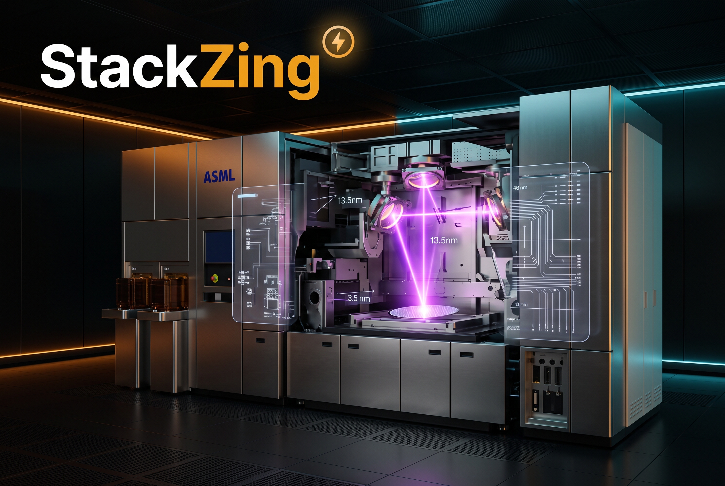
The modern artificial intelligence boom—from frontier multimodal models to the buildout of multi-gigawatt hyperscaler data centers—is widely treated as a software and algorithmic revolution. In reality, the entire global artificial intelligence economy is anchored to physical, atomic limits. Every leading-edge AI accelerator manufactured today—including NVIDIA’s Blackwell and Hopper architectures, AMD’s Instinct accelerators, Apple’s M-series silicon, Google’s TPUs, and Amazon’s Trainium chips—is impossible to produce without lithography equipment designed and assembled by a single company: ASML (Advanced Semiconductor Materials Lithography) in Veldhoven, Netherlands. ASML holds an absolute 100% commercial monopoly over Extreme Ultraviolet (EUV) lithography. Without their machines, commercial manufacturing at 5nm, 3nm, 2nm, and sub-2nm Angstrom nodes ceases worldwide.
1. The Illusion of Infinite Compute & The Rayleigh Criterion
The technology industry frequently discusses artificial intelligence as though compute were an abstract, infinitely scalable cloud resource. Venture capital flows into model training architectures, context-window expansions, and algorithmic optimizers under the implicit assumption that the underlying hardware will compound on schedule.
In reality, computational density is strictly bounded by the foundational mathematical law of optical photolithography—The Rayleigh Criterion:
For more than two decades, the semiconductor industry extracted performance gains by manipulating k₁ and NA using Deep Ultraviolet (DUV) argon fluoride immersion lasers operating at a wavelength of λ = 193 nanometers.
As transistor features shrank below 14nm, 193nm light became far too coarse. Trying to print a 7nm circuit feature with a 193nm light beam is physically equivalent to drawing a fine line using a wide paintbrush.
Foundries were forced into cumbersome, yield-destroying workarounds known as multi-patterning (Self-Aligned Quadruple Patterning, or SAQP). A wafer had to be exposed, etched, coated, and re-exposed up to four or eight times just to print a single layer of a chip. This caused manufacturing cycle times to balloon to over 20 weeks per wafer, drove defect rates skyward, and pushed fab economics to the brink of collapse.
To keep Moore’s Law alive and make modern AI compute possible, the industry had to radically reduce λ. ASML spent over two decades and tens of billions of dollars bypassing intermediate spectrum steps to commercialize Extreme Ultraviolet light at λ = 13.5 nanometers—a wavelength over 14 times shorter than DUV, residing on the threshold of soft X-rays.
2. The Violent Physics of 13.5nm EUV Generation
Unlike standard ultraviolet or visible light, 13.5nm EUV light cannot be produced by solid-state lasers, LEDs, or conventional gas discharge chambers. Producing commercial levels of EUV light requires one of the most violent, precisely synchronized thermodynamic reactions in industrial history.
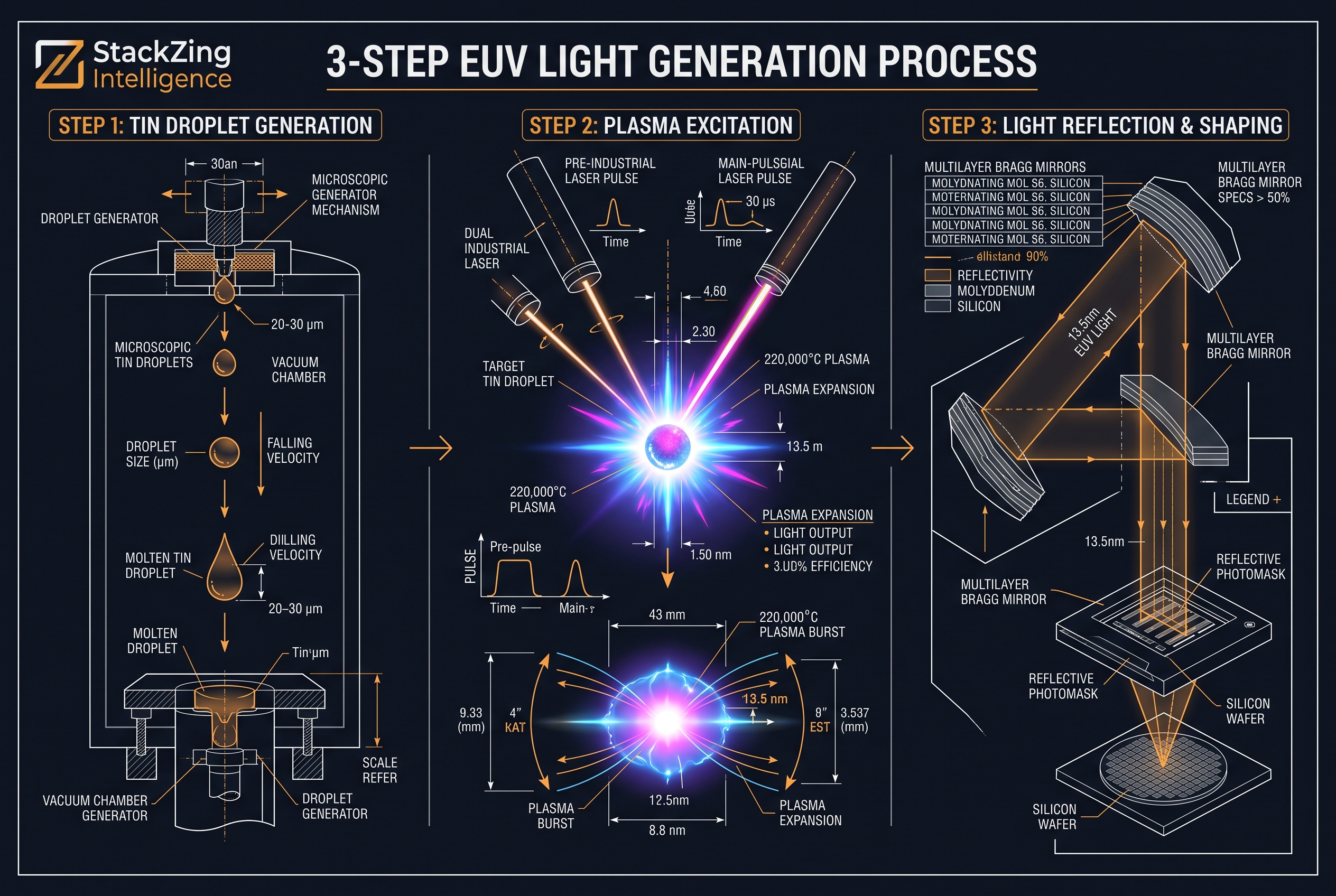
The 4-Step Tin Plasma Cycle (Repeated 50,000 Times Per Second)
Inside an ultra-high vacuum chamber at the base of an ASML Twinscan NXE scanner, the following cycle occurs continuously:
If a single laser pulse misfires by even a few nanoseconds, or if a tin droplet's trajectory deviates by a single micron, the plasma collapses, photon output drops to zero, and the silicon exposure process fails immediately.
3. Carl Zeiss & The Smoothest Mirrors in Human History
Once 13.5nm light is generated, it introduces a severe physical complication: EUV light is absorbed by almost all matter.
EUV cannot travel through air (requiring the entire multi-ton scanner to operate in a high vacuum), nor can it pass through traditional glass lenses. The moment 13.5nm photons strike conventional optical glass, they are absorbed and converted into waste heat.
To direct, shape, and focus EUV light onto silicon wafers, ASML partnered exclusively with Carl Zeiss SMT in Oberkochen, Germany, to develop specialized Multilayer Bragg Reflective Optics.
Zeiss constructs these mirrors by depositing 40 to 50 alternating bilayers of molybdenum and silicon onto ultra-low expansion glass-ceramic substrates. Each layer is measured in single-digit nanometers to ensure constructive wave interference.
The surface tolerances are measured in picometers. If a Zeiss EUV projection mirror were scaled to the geographical size of Germany, the highest bump or imperfection on the entire surface would be less than 1 millimeter high.
Despite this atomic perfection, each mirror reflection absorbs roughly 30% of the light. Because an EUV scanner requires between 10 to 12 successive mirror reflections to route the beam from the source, through the photomask, and down through the projection optics, less than 2% to 4% of the original light energy reaches the photoresist layer on the silicon wafer.
This optical tax explains why ASML must generate an overwhelmingly violent plasma source: to ensure that enough photons reach the wafer to maintain commercial fab throughput (typically 150 to 200 wafers per hour).
Never Miss an Executive Tech & Macro Teardown
Join 5,000+ technology leaders, portfolio managers, and independent specialists receiving our daily 5-minute morning intelligence brief. Zero fluff. High-signal analysis.
Subscribe Free at thestackzing.com →4. Entering the Angstrom Era: 0.33 Low-NA vs. 0.55 High-NA EUV
To manufacture chips at the 2nm, 1.4nm (TSMC A16, Intel 14A), and sub-1nm nodes required for future generations of AI accelerators, standard 0.33 NA EUV systems are reaching their physical resolution limit.
In response, ASML has deployed its next-generation platform: High-NA EUV (Twinscan EXE Series).
By boosting the lens Numerical Aperture from 0.33 to 0.55, High-NA EUV provides a 1.7x resolution boost, shrinking printable features down to 8nm in a single exposure.
The Anamorphic Reticle Revolution
High-NA EUV introduced a fundamental optical challenge: increasing the lens angle meant light struck the photomask at such steep angles that the light would be blocked by the mask's own 3D absorber patterns.
To solve this, ASML and Zeiss developed Anamorphic Optics. The system magnifies the mask pattern by 4x in the horizontal direction and 8x in the vertical direction. This preserves optical fidelity but cuts the standard exposure field (the "reticle size") in half.
As a result, chip design teams at NVIDIA, Apple, and Qualcomm must adapt their floorplanning tools (working with Synopsys and Cadence) to design larger AI processors across split reticle fields without losing interconnect speed.
5. The Hardware Hierarchy: From ASML Cleanrooms to NVIDIA Blackwell
The commercial journey of an artificial intelligence accelerator traces a direct, unbroken line from specialized supplier workshops in Western Europe to hyperscaler server racks in North America and Asia.

The 5-Step Compute Value Chain:
- Tier-1 Sub-System Monopolies: Carl Zeiss SMT builds the Bragg mirror blocks; Trumpf supplies high-power industrial CO₂ drive lasers; Cymer (an ASML subsidiary) engineers the high-frequency droplet chamber.
- System Integration (ASML): In Veldhoven, Netherlands, ASML integrates over 100,000 discrete components, 3,000 cabling harnesses, 40,000 precision fasteners, and multiple cleanroom modules into a single Twinscan scanner.
- Leading-Edge Wafer Fabrication: The scanners are shipped to top foundries—primarily TSMC (Fabs 18 and 20 in Taiwan), alongside Intel and Samsung. Foundries run raw 300mm silicon wafers through hundreds of sequential lithography, etching, ion implantation, and chemical-mechanical polishing (CMP) cycles.
- Advanced 2.5D/3D Packaging (CoWoS): Once the wafers are sliced into dies, pure lithography reaches its reticle boundary. TSMC mounts the compute dies alongside High-Bandwidth Memory (HBM3e/HBM4) onto high-density silicon interposers using CoWoS (Chip-on-Wafer-on-Substrate) packaging.
- Data Center Deployment: The completed accelerator modules (e.g., NVIDIA GB200 NVL72 rack-scale systems) are delivered to cloud hyperscalers to power the training and inference clusters of frontier AI labs.
6. The Single Point of Failure: Fragility and Geopolitics
The entire global technology infrastructure is built upon an extraordinarily concentrated physical foundation. This concentration introduces three distinct vulnerabilities:
7. The Economic Moat: Foundry CapEx and the Silicon Treadmill
The escalating cost of extreme lithography has fundamentally altered the economics of the semiconductor industry.
During the 1990s, dozens of integrated device manufacturers (IDMs) operated leading-edge semiconductor fabrication facilities worldwide. As the physics of lithography grew more complex and capital costs climbed exponentially, the field consolidated rapidly:
- 2002 (130nm Node): 25+ Leading-Edge Foundries Globally
- 2014 (14nm Node): 4 Foundries (TSMC, Intel, Samsung, GlobalFoundries)
- 2026 (2nm / High-NA Era): 3 Foundries (TSMC, Intel, Samsung)
At $380 Million to $400+ Million per High-NA scanner, outfitting a single modern fabrication facility with a production fleet of 15 to 20 machines requires an upfront capital investment exceeding $15 Billion to $20 Billion for the lithography tools alone—before accounting for cleanroom construction, chemical etching tools, metrology systems, and advanced packaging lines.
This capital intensity creates a self-reinforcing economic moat:
- Foundries must operate at 85% to 90%+ capacity utilization around the clock simply to amortize the depreciation of their ASML fleet.
- Only three companies on Earth—TSMC, Samsung, and Intel—have balance sheets capable of supporting this level of sustained capital expenditure.
- Hyperscalers (Microsoft, Alphabet, Amazon, Meta) must allocate tens of billions of dollars annually to secure foundry allocation years in advance, effectively underwriting ASML’s multi-year forward order book.
The Strategic Verdict
The artificial intelligence supercycle is not floating freely in the digital cloud. It is anchored to the physical world—bounded by the speed of light, thermal plasma dynamics, atomic mirror tolerances, and the precision assembly cleanrooms of Veldhoven. While researchers continue to invent novel model architectures, optimize transformer attention mechanisms, and develop more efficient software kernels, their work is ultimately governed by the number of transistors that can be printed per square millimeter of silicon. For the next decade, the computational ceiling of human civilization will continue to pass through a single, irreplaceable aperture: the optical path of an ASML scanner.
Master Enterprise Tech, Semiconductors & Global Macro
Join thousands of technology executives, investors, and independent specialists receiving our free 5-minute morning intelligence brief. Direct data, actionable frameworks, zero fluff.